Analyzing the Shift Toward High-Performance Computing and Its Requirements for the Global Semiconductor Wafer Market
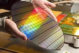
The current discourse in the tech industry revolves around the rapid advancement of Artificial Intelligence and its massive appetite for processing power, which in turn drives the semiconductor wafer market. High-performance computing (HPC) clusters and data centers require millions of high-end GPUs and CPUs, all of which start their journey as high-grade silicon wafers. The focus has shifted toward producing wafers that can support "chiplet" architectures, where multiple smaller dies are integrated into a single package. This trend requires wafers with exceptional structural integrity and thermal conductivity to handle the heat generated by densely packed circuits. As a result, we are seeing an increased interest in specialized polishing techniques, such as Chemical Mechanical Planarization (CMP), which ensures that the wafer surface is perfectly flat for multi-layer metal interconnects. The ability of the wafer market to provide these high-spec substrates is the primary bottleneck for the next generation of supercomputers and AI training models.
The global landscape is also reacting to the shifting patterns of electronic consumption, where emerging markets are becoming major players in the assembly and testing phases. The Semiconductor Wafer Market trends show a clear trajectory toward diversifying the manufacturing base to include regions with lower operational costs but high technical expertise. This globalization is accompanied by a drive for digitalization within the factories themselves, often referred to as Industry 4.0. Smart factories use real-time data to monitor every stage of wafer production, from the initial crystal growth to the final inspection, allowing for predictive maintenance and significantly higher yields. As the industry moves toward 2nm and 1.4nm nodes, the precision required will reach the atomic level, making the wafer the most critical component in the entire electronics value chain. The coming years will likely see a flurry of mergers and acquisitions as companies seek to consolidate their IP and manufacturing footprints to dominate this essential sector.
Frequently Asked Questions
-
How does AI influence the demand for semiconductor wafers? AI requires specialized chips with high transistor counts and efficient power delivery, which increases the demand for the highest quality 300mm wafers.
-
What is Chemical Mechanical Planarization (CMP)? CMP is a process used in semiconductor manufacturing to smooth the surface of the wafer using a combination of chemical etching and mechanical polishing.